
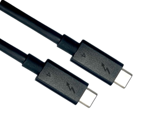
Poor connections in USB Cable Assembly often result from stress on solder joints, conductor fatigue and contact deterioration. Prevention during design starts with strain relief and the selection of suitable cables and contacts.
Six months after shipment, customer complaints begin to arrive: the USB cable works intermittently. On disassembly, the break is repeatedly found in the short section just behind the connector. Does this sound familiar? More frustratingly, every cable in the same batch passed prototype testing. Why did the problems appear only after the cables reached users?
These failures develop over time. Repeated bending, pulling and mating gradually cause solder joints and conductors to loosen or fracture. Waiting until mass production to modify the mould means incurring tooling costs again and extending the delivery schedule!
Matching failure modes to design measures can reduce many risks of poor contact before drawings are released.
Four Common Failure Modes Behind Poor Connections in USB Cable Assembly
Poor connections in USB Cable Assembly can be grouped into four categories: solder joint failure, conductor breakage, contact deterioration and assembly process variation. Each occurs in different locations, produces different symptoms and requires different preventive measures.
| Failure mode | Location | Typical symptoms | Main causes |
|---|---|---|---|
| Cracked solder joint or incomplete solder connection | Solder joint between the conductor and plug contact | Intermittent signals or interrupted charging when the cable is moved | Pulling and bending loads acting directly on the joint or insufficient wetting during soldering |
| Conductor fatigue and breakage | Bending point just beyond the boot exit | Disconnection only at a particular bending angle with no visible external damage | Repeated sharp bending at the same point, breaking copper strands progressively |
| Contact deterioration | Mating interface between plug and receptacle | Operation only when pressure is applied to the connector; elevated contact resistance | Plating wear exposing underlying material to oxidation or loss of spring contact force through stress relaxation or fatigue |
| Assembly process variation | Stripping, soldering and moulding operations | Isolated defects within a batch that may be difficult to reproduce | Loose conductor strands, misalignment during soldering or jacket deformation caused by heat or clamping |
A common situation is that latent defects in the first two categories may escape initial continuity testing and appear only after a period of use. These cases can therefore be dismissed as “improper user handling”. Start by locating the failure. If it is in the short section behind the connector, first check stress distribution and soldering quality. If the problem is at the mating interface, check the contact specification, wear and contamination.
Cable Exits and Solder Joints: How to Design Strain Relief
Strain relief is intended to make the cable jacket and moulded material carry most of the load when users pull or bend the cable, reducing the load transmitted to solder joints and conductors. In practice, three areas can be addressed:
- Secure the cable before the solder joints: Add an inner mould or clamping structure outside the soldering area to secure the cable to the plug body and reduce the axial pulling force acting directly on the solder joints.
- Provide a gradual transition in boot bending stiffness: Design the moulded boot at the cable exit by considering material hardness, thickness and shape together. Bending stiffness should transition smoothly from the plug body towards the cable. Segmented ribs or grooves at the end can distribute bending along a smooth curve and prevent it from concentrating at a single point.
- Secure the boot to the jacket: Join the boot to the cable jacket through overmoulding or a mechanical interlock so that the two do not slide independently under tension and the conductors do not carry the entire pulling load.
The dimensions of the plug and outer moulding affect the space available for the inner mould. USB Type-A Connector plugs have a larger shell cross section, generally providing more room for inner moulding and clamping structures. USB Type-C Connector and Micro USB Connector plugs have smaller shells. USB Type-C requirements also limit plug overmould width and height, so boot dimensions and inner mould geometry should be reviewed early in the design process.
For products used outdoors or in humid environments, consider a Waterproof USB Connector on the device side. On the cable side, the moulded material should fully cover the cable exit and the interfaces between materials must seal properly to reduce the risk of moisture entering along the jacket interface and accelerating contact corrosion. Waterproof performance must still be verified under the actual assembly and mating conditions.
A Prevention Checklist for Contact Selection, Cable Selection and Prototype Validation
Contact and cable selection affect the service life of the mating interface and the number of bending cycles the conductors can withstand. Requirements for these items can be established when specifications are prepared. Check the following five points during design review:
- Match rated mating cycles to usage frequency: Datasheets for USB Type-A Connector, USB Type-C Connector and Micro USB Connector products specify their rated mating cycles. First estimate the actual number of mating cycles over the product lifetime, then confirm that the selected connector provides sufficient margin.
- Specify plating type and thickness: Gold plated contacts with a nickel underlayer offer good resistance to oxidation. Wear resistance, however, depends on plating type, thickness and contact force. Applications involving frequent mating should specify these details explicitly instead of simply stating “gold plated”.
- Match conductor stranding to bending requirements: For cables that must bend repeatedly, consider stranded conductors with more, finer strands. However, flex life also depends on lay length, overall cable construction and bend radius. Confirm performance through bending tests representative of actual use rather than judging it by strand count alone.
- Include soldering conditions in the assembly specification: Strip length, conductor preparation, soldering temperature and heating time all affect solder joint quality. Documenting these in the assembly specification helps maintain consistency between batches.
- Perform bending and tensile tests during prototyping: In addition to continuity testing, subject samples to repeated bending and axial pulling based on actual use. Monitor for momentary discontinuities during bending and measure contact resistance or cable assembly resistance before and after testing using the specified method. Acceptance criteria should follow the product specification for discontinuities and the relevant resistance limit or permitted increase.
If any of these five points still lacks the relevant specified values before drawings are released, it represents an unresolved risk. Address each item during the design review.
Frequently Asked Questions
Q: How can you tell whether a poor USB connection is caused by the cable or the receptacle?
A: Cross checking can help narrow down the source of a poor USB connection. With device, power supply and transfer mode conditions kept consistent and confirmed to be working, a cable that still fails in another working receptacle is more likely to be at fault. If a compatible cable known to work also fails in the original receptacle, investigate the receptacle and device. To narrow down a cable fault, hold the connector still and bend only the cable. Signal loss near the cable exit often indicates broken conductors or stress on a solder joint. If signal loss occurs only when the insertion angle changes, the contact surface or spring contact is more likely to be involved.
Q: When does a USB cable need overmoulding?
A: Overmoulding is suitable when a USB cable will be repeatedly bent, mated or pulled. When the moulding compound and jacket materials are compatible, overmoulding can join the boot and jacket into an integrated structure that distributes bending stress over a longer section. If the cable follows a fixed internal route and does not move after assembly, a simple boot or clamping structure is usually sufficient. The key is to confirm that the cable route does not create a sharp bend just behind the connector.
Q: How much change in contact resistance indicates that a USB contact has deteriorated?
A: Assess USB contact deterioration against the contact resistance limit or permitted increase in the specification. No single value applies to every model. During prototyping, measure initial contact resistance using the specified method, repeat the measurement after durability testing and check both the absolute value and the increase against the specification. If the measurement covers the entire cable assembly, assess it against the corresponding specification; it cannot be treated as the contact resistance of a single contact. A sample that exceeds the permitted increase fails even if it still passes continuity testing because abnormal resistance can increase the risk of voltage drop, heating or intermittent connections.
USB Cable Assembly: Many Poor Contact Risks Can Be Reduced During Design
Poor connections in USB Cable Assembly are often associated with insufficient stress distribution or contact and cable specifications that do not match actual use. Both can still be addressed at the drawing stage. Start by defining four conditions: interface type, expected mating frequency, cable bending pattern and operating environment. Then check these against the selection and prototype validation checklist.
Walta Electronic has provided cable assembly services since 2014. As a Cable Assembly Manufacturer operating on an OEM/ODM basis, we provide support from product design, tooling development, prototyping and testing through to mass production. Please call us or email your specification requirements to discuss your needs.
Walta Electronic
Tel: 886-2-2657-7778
Email: inquiry@walta.com.tw
Address: 3F-2, No. 15, Lane 360, Section 1, Neihu Road, Neihu District, Taipei City, Taiwan